


 Marcy’s Musings: The ‘Magic’ of Additive Processes
 It’s Only Common Sense: More Great Business Ideas from ‘Breaking Bad’
 Material Insight: The Dielectric Constant of PCB Materials
Analog Devices Further Strengthens its South-East Asia Operations with New Singapore Facility
May 31, 2023 | ACN NewswireEstimated reading time: 2 minutes
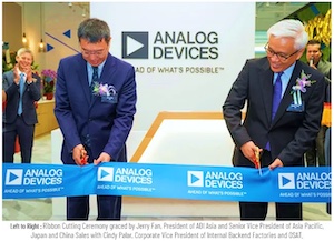
Analog Devices, Inc., a global semiconductor leader, announced the launch of a new state-of-the-art, environmentally friendly, 38,951 sq. ft. facility in Singapore. Located within the Kallang Industrial Park, the facility is planned to serve as a central hub for the more than 200 employees working in Singapore in key divisions of the company, including research and development, test engineering, sales, and manufacturing. ADI established its first location in Singapore in 1995 and has steadily grown its operations and workforce since then. This new strategic investment aligns with the company's global expansion plans, which include enhancing its capabilities in the Asia Pacific region.
"Our new facility is an important milestone in ADI's global growth strategy," said Jerry Fan, President of Asia for ADI. "Enhancing our capabilities in Singapore is vital to leveraging the country's superb talent pool and advanced manufacturing capabilities to serve our regional and global customers' needs. Our investment reinforces ADI's presence within Singapore's thriving semiconductor ecosystem, which is supported by the nation's digital growth initiatives."
The new facility features a more spacious and advanced laboratory to foster interaction between the research and development team as well as customers in the region. Through this forum for the exchange of ideas, ADI and its customers plan to deepen their collaboration and deliver innovative products for the Intelligent Edge. In addition, a dedicated space has been allocated for test development purposes within the new facility, custom-tailored to accommodate multiple automated test equipment (ATE) stations. These on-site testing stations are designed to enable faster initial testing of ADI's state-of-the-art products and accelerate the timeline of ADI engineering's ability to meet customers' toughest challenges.
Fan continued, "Customer intimacy, business strategy, engineering processes, manufacturing capabilities, and problem-solving are essential for creating long-term value for our customers. We are confident the environment within our new facility will help us deliver the kind of innovation that leads to breakthrough products and services, and we believe it will have a lasting impact on the region's ongoing digital transformation journey."
Location selection and build criteria for the site prioritized accessibility and sustainability. The new office is bicycle-friendly, close to public transportation, and is directly accessible via expressways. Recyclable materials were used throughout construction, and energy efficient AC, lighting, and water systems are all part of its advanced building automation system. Low carbon footprint materials were an integral part of the biophilic interior design. The office building is Green Mark Platinum-certified and expected to get LEED Gold certification by July 2023.
Share on:


Suggested Items
Advocacy: There’s No Time to Waste
05/21/2024 | Marcy LaRont, PCB007 MagazineIn the late 1990s, I worked for a PCB company ardently working to build manufacturing presences in Malaysia, Taiwan, and eventually China’s mainland. For some of us who had the resources, we followed our OEM customers offshore as they began demanding increasingly greater price concessions from their stateside suppliers. The government was not coming to the rescue of the PCB manufacturer, so we rode the changing economic tide as it turned unwaveringly toward globalism and cheaper labor.
Marcy’s Musings: The ‘Magic’ of Additive Processes
05/21/2024 | Marcy LaRont -- Column: Marcy's MusingsThough modern semi-additive and fully additive technologies are still emerging for PCB manufacturing, additive technology itself is not new. Many PCB fabricators find themselves at a crossroads when deciding whether to change their current processes and go additive or stay the course until something significant compels a change. But change is on the horizon, and it seems to be driven by significant technological advancements in chips and advanced packaging, offering PCB fabricators some additive manufacturing solutions to explore.
Real Time with… IPC APEX EXPO 2024: Custom PCB Solutions With Adura
05/20/2024 | Real Time with...IPC APEX EXPOColumnist Dan Beaulieu and Sumit Tomar, CEO of Adura, discuss the company's comprehensive manufacturing of custom PCBs. The company excels in thermal PCB technology for enhanced conductivity. As Sumit explains, they also plan to venture into power management, leveraging their U.S.-based manufacturing capabilities.
Zentech First to Adopt IPC Apprenticeship National Program Standards
05/20/2024 | Cory Blaylock, IPCIPC achieved a landmark in 2023 by creating an apprenticeship program approved by the U.S. Department of Labor. With such a registered framework in place, industry can work through IPC to secure local, state, and federal dollars for workforce development in a way they’ve never been able to do before. Zentech Manufacturing, headquartered in Baltimore, Maryland, with production facilities in Bloomington, Illinois, and Richardson, Texas, is the first employer partner to adopt IPC’s national program. Click here to read their story.
Danutek Celebrates 20 Anniversary
05/20/2024 | DanutekDanutek, a leading supplier of capital equipment and service support to the electronics manufacturing sector in Europe, proudly marks its 20th anniversary this year.