


 Marcy's Musings: The Growing Industry
 It’s Only Common Sense: Here’s What To Do After IPC APEX EXPO 2024
 Dan’s Biz Bookshelf: Seeing the How
Synthesizing Single-Crystalline Hexagonal Graphene Quantum Dots
August 6, 2019 | KAISTEstimated reading time: 2 minutes
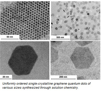
A KAIST team has designed a novel strategy for synthesizing single-crystalline graphene quantum dots, which emit stable blue light. The research team confirmed that a display made of their synthesized graphene quantum dots successfully emitted blue light with stable electric pressure, reportedly resolving the long-standing challenges of blue light emission in manufactured displays. The study, led by Professor O Ok Park in the Department of Chemical and Biological Engineering, was featured online in Nano Letters on July 5.
Graphene has gained increased attention as a next-generation material for its heat and electrical conductivity as well as its transparency. However, single and multi-layered graphene have characteristics of a conductor so that it is difficult to apply into semiconductor. Only when downsized to the nanoscale, semiconductor’s distinct feature of bandgap will be exhibited to emit the light in the graphene. This illuminating featuring of dot is referred to as a graphene quantum dot.
Conventionally, single-crystalline graphene has been fabricated by chemical vapor deposition (CVD) on copper or nickel thin films, or by peeling graphite physically and chemically. However, graphene made via chemical vapor deposition is mainly used for large-surface transparent electrodes. Meanwhile, graphene made by chemical and physical peeling carries uneven size defects.
The research team explained that their graphene quantum dots exhibited a very stable single-phase reaction when they mixed amine and acetic acid with an aqueous solution of glucose. Then, they synthesized single-crystalline graphene quantum dots from the self-assembly of the reaction intermediate. In the course of fabrication, the team developed a new separation method at a low-temperature precipitation, which led to successfully creating a homogeneous nucleation of graphene quantum dots via a single-phase reaction.
Professor Park and his colleagues have developed solution phase synthesis technology that allows for the creation of the desired crystal size for single nanocrystals down to 100 nano meters. It is reportedly the first synthesis of the homogeneous nucleation of graphene through a single-phase reaction.
Professor Park said, "This solution method will significantly contribute to the grafting of graphene in various fields. The application of this new graphene will expand the scope of its applications such as for flexible displays and varistors.”
This research was a joint project with a team from Korea University under Professor Sang Hyuk Im from the Department of Chemical and Biological Engineering, and was supported by the National Research Foundation of Korea, the Nano-Material Technology Development Program from the Electronics and Telecommunications Research Institute (ETRI), KAIST EEWS, and the BK21+ project from the Korean government.
Share on:


Suggested Items
Insulectro’s 'Storekeepers' Extend Their Welcome to Technology Village at IPC APEX EXPO
04/03/2024 | InsulectroInsulectro, the largest distributor of materials for use in the manufacture of PCBs and printed electronics, welcomes attendees to its TECHNOLOGY VILLAGE during this year’s IPC APEX EXPO at the Anaheim Convention Center, April 9-11, 2024.
ENNOVI Introduces a New Flexible Circuit Production Process for Low Voltage Connectivity in EV Battery Cell Contacting Systems
04/03/2024 | PRNewswireENNOVI, a mobility electrification solutions partner, introduces a more advanced and sustainable way of producing flexible circuits for low voltage signals in electric vehicle (EV) battery cell contacting systems.
Heavy Copper PCBs: Bridging the Gap Between Design and Fabrication, Part 1
04/01/2024 | Yash Sutariya, Saturn Electronics ServicesThey call me Sparky. This is due to my talent for getting shocked by a variety of voltages and because I cannot seem to keep my hands out of power control cabinets. While I do not have the time to throw the knife switch to the off position, that doesn’t stop me from sticking screwdrivers into the fuse boxes. In all honesty, I’m lucky to be alive. Fortunately, I also have a talent for building high-voltage heavy copper circuit boards. Since this is where I spend most of my time, I can guide you through some potential design for manufacturability (DFM) hazards you may encounter with heavy copper design.
Trouble in Your Tank: Supporting IC Substrates and Advanced Packaging, Part 5
03/19/2024 | Michael Carano -- Column: Trouble in Your TankDirect metallization systems based on conductive graphite or carbon dispersion are quickly gaining acceptance worldwide. Indeed, the environmental and productivity gains one can achieve with these processes are outstanding. In today’s highly competitive and litigious environment, direct metallization reduces costs associated with compliance, waste treatment, and legal issues related to chemical exposure. What makes these processes leaders in the direct metallization space?
AT&S Shines with Purest Copper on World Recycling Day
03/18/2024 | AT&SThe Styrian microelectronics specialist AT&S is taking World Recycling Day as an opportunity to review the progress that has been made in recent months at its sites around the world in terms of the efficient use of resources: