


 The Right Approach: I Hear the Train A Comin'
 It’s Only Common Sense: OCCAM—the Time Is Now
 Marcy's Musings: The Growing Industry
Samsung Adopts Ansys' Simulation Portfolio to Create Semiconductor Designs to Optimize High-Speed Connectivity
July 7, 2022 | ANSYSEstimated reading time: 1 minute
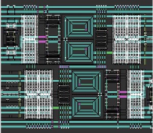
Samsung Foundry will engage Ansys' industry-leading electromagnetic (EM) simulation tools to develop ultramodern designs, including 5G/6G, on the most advanced chips, nodes, and process technologies. Ansys' simulation solutions will deliver a comprehensive EM-aware design flow with greater capacity, speed, and integration capabilities for Samsung's most advanced semiconductor technology, accelerating on-chip design cycle times to boost high-speed connectivity while helping to reduce design error and risk.
Samsung designers will leverage Ansys' EM design tools, Ansys RaptorX, Ansys VeloceRF, and Ansys Exalto, to help reduce time to market by two to three weeks on smaller designs and up to two months for complex designs. With automation capabilities that optimize calculations and modeling, coupled with larger capacity, Ansys' software will allow the Samsung team to design at faster speeds with higher fidelity.
"Electronic systems and process technologies are constantly evolving and therefore require leading-edge EM design capabilities," said Sangyun Kim, corporate vice president of the Foundry Design Technology Team at Samsung Electronics. "We believe that Ansys' simulation solutions meet these challenges and will deliver the highest level of proficiency for our design needs, while reducing design time, cost, and risk."
By integrating Ansys' EM solutions, Samsung designers can model complex on-chip scenarios, including dummy tiles, which comprise millions of metal pieces in a fraction of the time. Additionally, Ansys' near real-time modelling capabilities safeguard designs from EM interference, which helps significantly lower the risk of chip failure.
"EM is a primary challenge for chip designers as connectivity demands increase and technologies advance worldwide," said John Lee, vice president and general manager of the electronics, semiconductor, and optics business unit at Ansys. "At Ansys, we ensure that our simulation solutions not only meet these rising demands but remain ahead of them. We are confident that Ansys' EM design portfolio is well-equipped to serve the Samsung team with the tools they need to optimize their on-chip designs."
Ansys and Samsung have a long history of collaboration that delivers advanced solutions, including power integrity and electromigration signoff solutions for low-power mobile and high-performance computing applications.
Share on:


Suggested Items
Cadence, TSMC Collaborate on Wide-Ranging Innovations to Transform System and Semiconductor Design
04/25/2024 | Cadence Design SystemsCadence Design Systems, Inc. and TSMC have extended their longstanding collaboration by announcing a broad range of innovative technology advancements to accelerate design, including developments ranging from 3D-IC and advanced process nodes to design IP and photonics.
Ansys, TSMC Enable a Multiphysics Platform for Optics and Photonics, Addressing Needs of AI, HPC Silicon Systems
04/25/2024 | PRNewswireAnsys announced a collaboration with TSMC on multiphysics software for TSMC's Compact Universal Photonic Engines (COUPE). COUPE is a cutting-edge Silicon Photonics (SiPh) integration system and Co-Packaged Optics platform that mitigates coupling loss while significantly accelerating chip-to-chip and machine-to-machine communication.
Siemens’ Breakthrough Veloce CS Transforms Emulation and Prototyping with Three Novel Products
04/24/2024 | Siemens Digital Industries SoftwareSiemens Digital Industries Software launched the Veloce™ CS hardware-assisted verification and validation system. In a first for the EDA (Electronic Design Automation) industry, Veloce CS incorporates hardware emulation, enterprise prototyping and software prototyping and is built on two highly advanced integrated circuits (ICs) – Siemens’ new, purpose-built Crystal accelerator chip for emulation and the AMD Versal™ Premium VP1902 FPGA adaptive SoC (System-on-a-chip) for enterprise and software prototyping.
Listen Up! The Intricacies of PCB Drilling Detailed in New Podcast Episode
04/25/2024 | I-Connect007In episode 5 of the podcast series, On the Line With: Designing for Reality, Nolan Johnson and Matt Stevenson continue down the manufacturing process, this time focusing on the post-lamination drilling process for PCBs. Matt and Nolan delve into the intricacies of the PCB drilling process, highlighting the importance of hole quality, drill parameters, and design optimization to ensure smooth manufacturing. The conversation covers topics such as drill bit sizes, aspect ratios, vias, challenges in drilling, and ways to enhance efficiency in the drilling department.
Elevating PCB Design Engineering With IPC Programs
04/24/2024 | Cory Blaylock, IPCIn a monumental stride for the electronics manufacturing industry, IPC has successfully championed the recognition of the PCB Design Engineer as an official occupation by the U.S. Department of Labor (DOL). This pivotal achievement not only underscores the critical role of PCB design engineers within the technology landscape, but also marks the beginning of a transformative journey toward nurturing a robust, skilled workforce ready to propel our industry into the future.